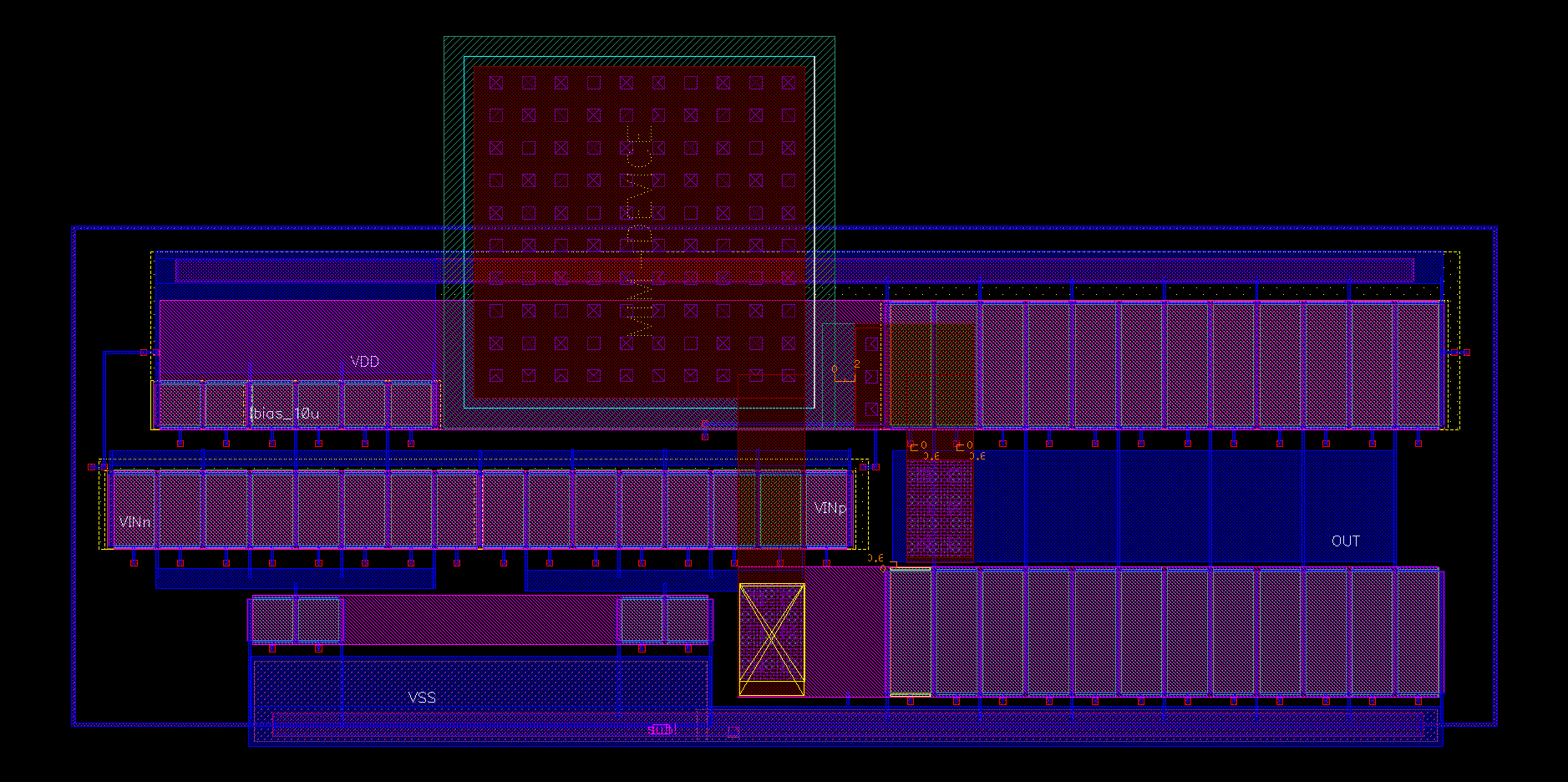
Fig. 1 Two Stage OTA Schematic
Finally, while most existing space heaters present users with numerous buttons and dials, OCTA simplifies its controls to three simple buttons and subtle LED temperature indicators. Red Dot Award: Design Concept | Concept | Domestic Aid. Through improved safety, simplified operation, and expressive home-friendly aesthetics, OCTA attempts to.
Typical fully differential OTA with source degeneration. (a)... Download Scientific Diagram
1,427. Re: OTA design step by step. these are some general steps for start: 1- if you have a limit for your power consumption, you can calculate your total allowalbe current (by knowing the value of your power supply). if not,assume a reasonable limit, maybe around 5-10mw for 1.8v power supply. 2- By writting the equations of Gain, settling.

Javed kitchen ota specialist.karanja lad YouTube
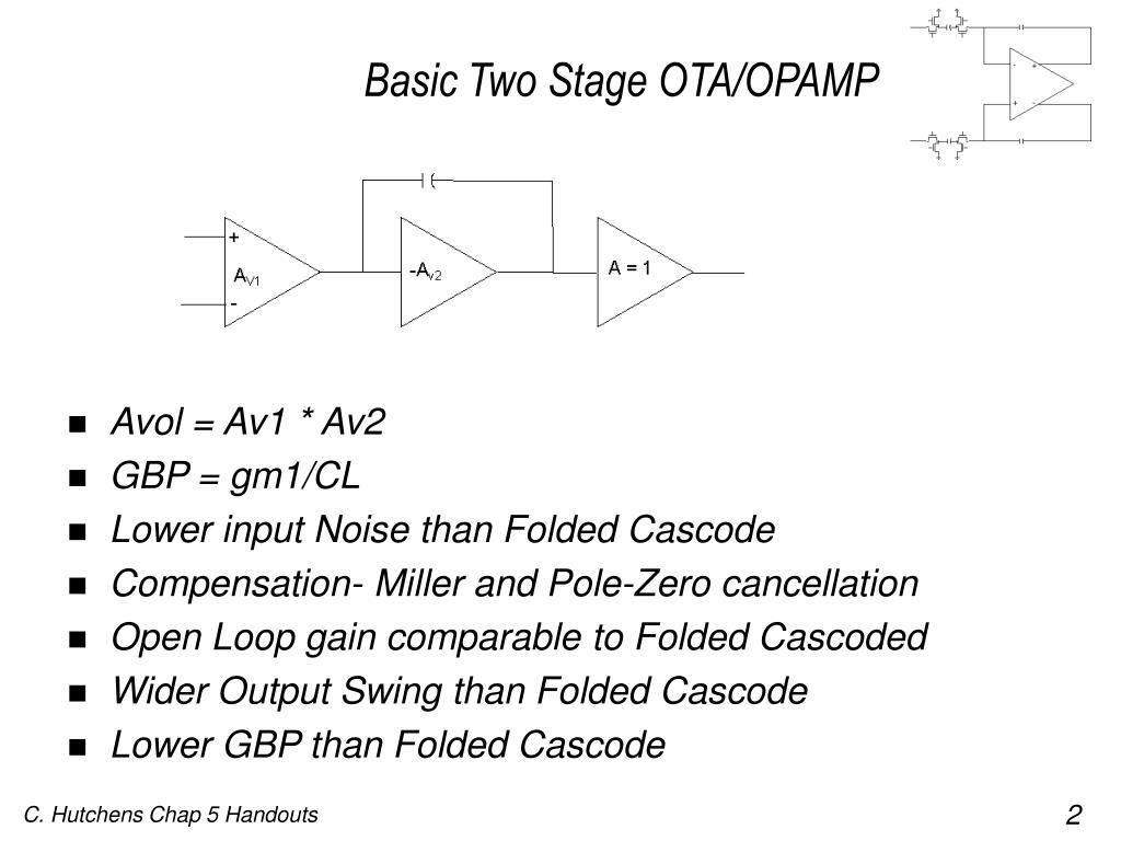
This chapter is devoted to simplified design with operational transconductance amplifiers, or OTAs. An OTA is similar to the op-amps described in Chapter 3. However, OTAs and op-amps are not always interchangeable. For that reason, an explanation of unique characteristics found in OTAs is in order. The OTA not only includes the usual.
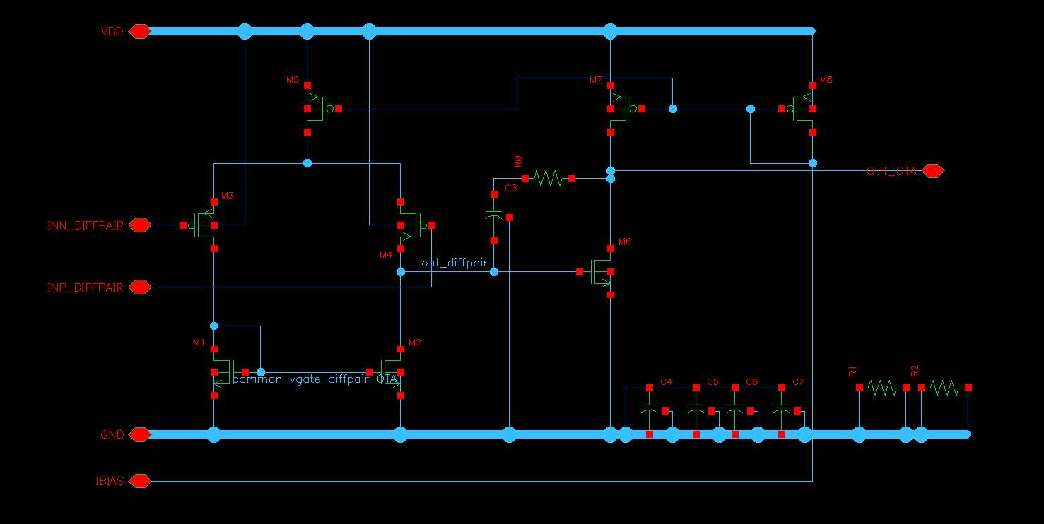
Figure 3. OTA Schematic
Design considerations for the interaction of the operation of common-mode feedback (CMF) and tuning are discussed, and improved CMF circuits are proposed. Using the GaAs OTA and considering the frequency limitations imposed by parasitics, the design of a high order ladder filter with 300MHz cutoff frequency is presented as an application.

Two stage OTA design (replicates the Schmitt trigger section of the... Download Scientific Diagram
Rounok Joardar. Abstract - This paper describes the design and simulation of a low-power two-stage operational transconductance amplifier (OTA) using a 0.18 m CMOS technology and a 1.8V power supply. It is shown that with careful design, a low-frequency gain greater than 70dB can be achieved together with high phase margin (greater than 45.

5TOTA Design and Simulation Using Cadence Virtuoso YouTube
Traditional analog design methodologies typically require iteration. "Square Law" design equations are inaccurate for submicron devices. Depend on poorly defined parameters: mCox, Vth, Vdsat,. Difficult to achieve an "optimum" (e.g. minimum power) gm/Id-based design. Links design variables (gm, ft, Id,.) to specification.

Analog VLSI Design Lecture 42.4 Two stage OTA design procedure YouTube
BYD overtook Tesla as the world's top seller of electric vehicles (EV) at the end of last year, crowning an extraordinary rise for the Chinese carmaker.

Kitchen Design,Small Kitchen Interior Design, Complete Kitchen Ota Design And Full Detail
Chris Savage, AIA, LEED AP, Principal. Chris is a Partner and Principal at RGA, Office of Architectural Design, Inc., a leader in the industrial sector in the Southern California market. He is licensed and LEED Accredited with two decades of experience in design, project management, and team leadership in development of state-of-the-art.

A Process Variation Tolerant OTA Design for Low Power ASIC Design
Transistors are transconductors. Some OTA designs consist of >40 transistors. Only few (typically 1. 2) provide the transconductance in the signal path. The rest is support, e.g. increasing low frequency gain. output voltage range. biasing. Hierarchical design strategies are imperative.
PPT OTA DESIGN and COMPENSATION PowerPoint Presentation ID402800
Reduced interaction between gain and output range. Somewhat higher drive capability for given C. in. Disadvantages. Increased power dissipation or reduced speed. Need for compensation. Examples: Miller-compensated 2-stage OTA. OTA with preamp (power efficiency?)
OTA(Overtheair)Introduction BenQ Business Europe
January 09, 2024 2:58 PM. Members of the Fort Worth Fire Department work the scene the morning after a massive explosion occurred at the Sandman Signature Hotel in downtown Fort Worth on Monday.

OvertheAir, OTA testing Everything you need to know Verkotan
Latest: Design may have prevented worse damage in downtown Fort Worth hotel explosion By Harriet Ramos. Updated January 09, 2024 4:06 PM. While natural gas did play some role, the city is.

Analog VLSI Design Lecture 42.1 Two stage OTA with singleended output YouTube
Two stage OTA design procedures @InderjitSingh87. AVLSI lecture 42.4 covers the following topics: 1. Two stage OTA design procedures @InderjitSingh87.

folded cascode ota design procedure hakatutorialwithlyrics
AVLSI lecture 37.4 covers the following topics: 1. Design of single stage OTA2. Estimation of aspect ratios for all transistors @InderjitSingh87

Two Stage Operational Transconductance Amplifier Design EEWeb
Design and Analysis of Self-biased OTA for Low-Power Applications G. Manikanta, R. A. Mishra, N. A. Srivastava and R. K. Jaiswal Abstract This paper presents an operational-transconductance-amplifier (OTA) for ultra-low power applications with high CMRR (common mode rejection ratio) and PSRR (power supply rejection ratio).
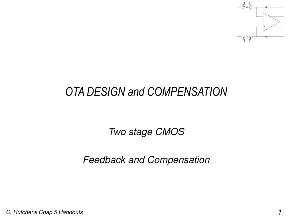
PPT OTA DESIGN and COMPENSATION PowerPoint Presentation, free download ID402800
Design considerations for the interaction of the operation of common-mode feedback (CMF) and tuning are discussed, and improved CMF circuits are proposed. Using the GaAs OTA and considering the frequency limitations imposed by parasitics, the design of a high order ladder filter with 300MHz cutoff frequency is presented as an application.